- English
- French
- German
- Portuguese
- Spanish
- Russian
- Japanese
- Korean
- Arabic
- Greek
- German
- Turkish
- Italian
- Danish
- Romanian
- Indonesian
- Czech
- Afrikaans
- Swedish
- Polish
- Basque
- Catalan
- Esperanto
- Hindi
- Lao
- Albanian
- Amharic
- Armenian
- Azerbaijani
- Belarusian
- Bengali
- Bosnian
- Bulgarian
- Cebuano
- Chichewa
- Corsican
- Croatian
- Dutch
- Estonian
- Filipino
- Finnish
- Frisian
- Galician
- Georgian
- Gujarati
- Haitian
- Hausa
- Hawaiian
- Hebrew
- Hmong
- Hungarian
- Icelandic
- Igbo
- Javanese
- Kannada
- Kazakh
- Khmer
- Kurdish
- Kyrgyz
- Latin
- Latvian
- Lithuanian
- Luxembou..
- Macedonian
- Malagasy
- Malay
- Malayalam
- Maltese
- Maori
- Marathi
- Mongolian
- Burmese
- Nepali
- Norwegian
- Pashto
- Persian
- Punjabi
- Serbian
- Sesotho
- Sinhala
- Slovak
- Slovenian
- Somali
- Samoan
- Scots Gaelic
- Shona
- Sindhi
- Sundanese
- Swahili
- Tajik
- Tamil
- Telugu
- Thai
- Ukrainian
- Urdu
- Uzbek
- Vietnamese
- Welsh
- Xhosa
- Yiddish
- Yoruba
- Zulu
In High-Precision DAQ - Architectural Analysis of The NI PXIe-4309
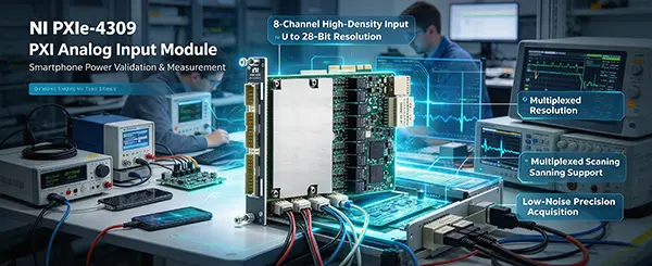
In semiconductor parameter characterization, large-scale lithium-battery microvolt-level monitoring, and high-density tactical aerospace instrumentation, maximizing the expansion of channel counts within a restricted module footprint while preserving extreme Analog-to-Digital Converter (ADC) conversion fidelity remains a key challenge for systems integrators. The NI PXIe-4309 is an elite 8-channel, 28-bit high-dynamic flexible resolution analog input module. However, when paired with hardware-level multiplexing expansion topologies, its variable architecture allows the physical input capacity to scale up to 32 channels. This article delivers a comprehensive engineering analysis of the sample rate balancing and channel settling time mechanics of the NI PXIe-4309 under multiplexed configurations. The discussion unfolds across critical technical dimensions—including multiplexer switched-capacitor charging/discharging modeling, maximum stable sampling rate trade-off equations across varying channel splits, zero-crosstalk differential grounding isolation layouts, and NI-DAQmx scan-list-based driver optimizations.
Orchestrating Deterministic Signal Integrity & Hardened Metrology Networks: The MXTD Engineering Standard
De-risk your mission-critical system deployment horizons and secure your strategic instrumentation boundaries by partnering with our international technical applications division at manager03@mxtdinfo.com or manager02@mxtdinfo.com. Contact our cross-functional engineering desk today to acquire accredited telemetry layouts, bespoke OEM platform specifications, or comprehensive physical-layer signal compliance audits.
Strategic Capabilities & Core Offerings
➡️ Accredited Telemetry Layouts: Validated circuit topologies and hardware schematics engineered for dense multi-channel integration and nanosecond-level edge determinism.
➡️ Bespoke OEM Platform Specifications: Hardened physical-layer electronics development and rugged enclosure design tailored to survive volatile, hyper-g mechanical shock and extreme thermal environments.
➡️ Physical-Layer Signal Compliance Audits: Comprehensive telemetry stress-testing and boundary verification to eradicate cross-talk, grounding isolation faults, and data drift at the absolute source.
The Core Conflict Between Channel Count and Timing in High-Density Precision Testing
When constructing high-density testing systems, the instrumentation goals regularly command a simultaneous expansion of both channel count and sample throughput. For instance, across large-scale Battery Management System (BMS) verification or complex multi-layer PCB voltage array monitoring, the topology must track dozens or hundreds of physical measurement points. If a dedicated, autonomous analog front-end and separate ADC are assigned to every single channel, the physical volumetric footprint and capital expenditure (CAPEX) of the system scale exponentially.
To circumvent this spatial and financial barrier, multiplexing techniques are heavily deployed. The NI PXIe-1088/4309 leverages an internal high-speed solid-state switch matrix, allowing multiple external physical pins to sequentially reference a single, high-precision 28-bit Delta-Sigma ADC core. However, integrating multiplexed topologies inherently introduces low-level temporal phase slicing constraints: as the number of scanned channels expands, the effective sampling rate apportioned per channel drops proportionally, and during fast channel switching, residual charge trapped on switched capacitors triggers severe channel-to-channel crosstalk and sampling distortion. Consequently, precisely balancing multiplexing parameters against sample rate throughput remains an uncompromised structural baseline during system integration.
Switched-Capacitor Modeling and Channel Settling Time in Multiplexed Architectures
[ Channel AI 0 Physical Pin ] ─── (Solid State Switch SW0) ──┐ ├──> [ Parasitic Capacitance C_stray + Instrumentation Amplifier C_in ] ──> [ 28-bit Precision ADC Core ] [ Channel AI 1 Physical Pin ] ─── (Solid State Switch SW1) ──┘ │ (Discharge Resistor R_bleed) │ [ Analog Ground Reference AI GND ]
Physical Layer Residual Charge and Crosstalk Mechanisms
When the NI PXIe-4309 18-28 Bit PXI Analog Input Module executes its scan list in multiplexed interface modes (such as 32-channel single-ended or 16-channel differential expansion topologies), the internal solid-state gates latch sequentially at microsecond-scale (\(\mu\text{s}\)) velocities. If the system has just completed the digitization of Channel 0 (resting at 10 V) and instantly breaks connection to latch Channel 1 (resting at 0.1 V), the stray parasitic capacitance (\(C_{\text{stray}}\)) across the multiplexed bus and the input capacitance (\(C_{\text{in}}\)) of the internal instrumentation amplifier will hold undissipated residual charge from Channel 0. If these charges fail to clear completely to analog ground (AI GND) prior to data latching, the initial potential read on Channel 1 will be artificially pulled high, macroscopically rendering severe cross-channel data contamination (crosstalk).
Impedance Calculations Governing Settling Time
To secure high-SNR, genuine raw potentials, the architecture must enforce an adequate Settling Time, ensuring residual charges decay through internal bleed resistances (\(R_{\text{bleed}}\)) down below the Least Significant Bit (LSB) quantization step of the target bit depth. For a 28-bit extreme resolution, the RC charge/discharge loop must cycle through at least 20 or more \(\tau \) (time constant) constants to compress the residual charge beneath one ten-millionth of its primary level. This imposes an uncompromised engineering redline: the output impedance of external field transducers must remain exceptionally low (strictly recommended under 10 \(\Omega \), or impedance-buffered via operational amplifier voltage followers). If the external source impedance is too broad (e.g., exceeding 1 k\(\Omega \)), the RC time constant elongates, driving the system into total distortion due to insufficient settling times under fast channel switching.
Multi-Channel Configurations and Sample Rate Trade-Off Matrix
The principal design of the NI PXIe-4309 18-28 Bit PXI Analog Input Module centers on flexible temporal scheduling. Because the aggregate hardware quantization throughput capacity of the internal ADC matrix is physically constrained, the total available sample rate is mathematically divided among the active channels inside the scan list. Systems engineers must rigidly adhere to the following channel-count vs. sample-rate trade-off matrix:
|
Configuration Mode |
Active Channels |
Max Stable Rate per Channel |
Effective Bit Depth per Channel |
Target Engineering Scenario |
|
Independent dedicated front end |
8 channels (AI 0 to AI 7) |
Full-speed independent decoupled parallel |
Highest speed transient dynamic waveform capture |
Powertrain torque sudden vibration, phased array radar coherent transient verification |
|
Multiplexed differential |
16 channels (multiplexed scanning) |
50 kS/s/ch (total throughput 800 kS/s) |
Balanced medium-speed dynamic capture |
Multi-axis mechanical structure complex fatigue life load stress comprehensive test chamber |
|
32-CH Multiplexed single-ended |
32 channels (full-slot high-density scanning) |
25 kS/s/ch (total throughput 800 kS/s) |
High-precision multi-point parallel online inspection |
Microvolt-level cell voltage group monitoring of large-scale new energy battery packs (BMS) |
|
Metrology Scan |
Arbitrary multiplexing extended channel |
Squeezing bandwidth through oversampling depth |
Extreme DC metering-grade precise nonlinear calibration |
Laboratory standard source nanovolt-level high dynamic voltage calibration and superconducting thermal drift analysis |
Software Driver Configuration and Scan-List Timing Fine-Tuning
To programmatically manage this multiplexed topology within the NI-DAQmx API while eliminating cross-channel crosstalk driven by insufficient capacitive charge bleeding, a three-layer soft-hardware co-optimization must be hardcoded during runtime initialization:
- Explicit Tuning of the Inter-Channel Conversion Clock (AI Convert Clock Rate): Upon creating a consolidated multi-channel DAQmx virtual task (e.g., spanning AI 0 through AI 31), developers must utilize driver attribute nodes to fine-tune the AI.Conv.Rate parameter. This underlying clock directly dictates the hardware dead-time anti-contention gap allowed between disconnecting the multiplexer from a prior channel and latching sample collection on the subsequent node. Sizing down this conversion frequency yields crucial microseconds of extra clear-and-discharge time for internal switched-capacitors.
- Implementing Strategic Spatial Channel Interleaving: When deploying physical terminal wiring layouts and defining the programmatic scan list, never continuously sequence a broad-swing ±10V signal channel (such as an industrial actuator output on AI 0) immediately adjacent to a microvolt-level μV fragile thermocouple trace (such as AI 1). Integrators should execute physical track isolation on the terminal breakout block or programmatically inject an intermediate grounded "buffer channel" into the DAQmx scan array, exploiting temporal interleaving to flatten physical-layer residual charges.
- Deactivating Soft Regeneration Modes to Secure FIFO Depth: Because continuous multiplexed scanning sequences generate accelerated, highly deterministic pulse streams, developers must execute DAQmx Configure Input Buffer calls to assign a RAM pool depth spanning at least 2-3 seconds of stream metrics. Coupling this setup with a high-priority Producer-Consumer multi-threaded thread architecture offloads data logging procedures to parallel independent CPU cores, protecting the backplane from temporal misalignment faults triggered by host OS freezes.
The NI PXIe-4309 18-28 Bit PXI Analog Input Module achieves system-level consolidation balancing expansive channel densities against extreme conversion fidelity within a compact single-module footprint by reconstructing programmable multiplexed control loops and 18-to-28-bit flexible dynamic decimation resolutions. Resolving the balanced trade-off between multiplexing parameters and sample rate throughput relies not on chasing isolated peak single-channel sampling frequencies, but on referencing the switched-capacitor charging/discharging model to constrain external transducer output impedances at the physical layer, deploy shielded twisted pairs, and programmatically balance conversion clock latencies and channel interleaving profiles via the NI-DAQmx driver layer. This closed-loop soft-hardware configuration guarantees that even under severe testing fields commanding continuous maximum-throughput 32-channel scanning, the instrumentation backbone thoroughly eliminates cross-channel crosstalk interferences, delivering zero-drift, high-SNR high-confidence digital instrumentation datasets.
References
National Instruments. (2025). NI PXIe-4309 Device Operating Instructions and Multi-Channel Multiplexing Calibration Reference Manual. Austin, TX: National Instruments.
National Instruments. (2026). Settling Time Mechanics, Switched-Capacitor Crosstalk, and Conversion Clock Configurations in Scanned High-Density Data Acquisition Platforms. Technical White Paper ID: DAQ-4309-99.
FAQs:
Q1: When I configure the PXIe-4309 to 32-channel single-ended scan mode and set the physical sampling rate to 25 kS/s/ch, why do some channels always have "residual shadow waveforms" of the amplitude-changing signals from adjacent channels superimposed on the fixed voltage waveforms? How can I eliminate this?
A1: This measurement artifact represents a highly frequent, multiplexer-specific engineering failure mode driven by incomplete capacitive charge dissipation, generating classic cross-channel crosstalk. Because all 32 channels sequentially multiplex a singular internal sampling capacitor at accelerated rates, if the electrostatic charge from a prior channel lacks adequate time to bleed down to zero through the reference resistance, its residual energy directly corrupts the sample read on the subsequent node, creating a "ghosting waveform" phantom. Eradicating this anomaly requires:
- Radically lower external source impedances: verify if the field sensor output impedance targeting the ghosting channel is too broad (if it exceeds a few hundred ohms, install an externally powered low-impedance operational amplifier voltage follower IC inline to force the source impedance beneath 10 Ω, accelerated capacitive charging);
- Scale down the AI Convert Clock Rate in your DAQmx configuration: programmatically insert an explicit idle discharge dead-time window spanning 10 μs to 50 μs between channel switching events;
- Deploy physical-layer shielded twisting: separate analog twisted-pair runs from high-frequency or high-voltage traces by a minimum of 15 cm of safe physical layout distance.
Q2: Since multiplexing scanning leads to a reduction in sampling rate and bit resolution, should I always choose the fully decoupled independent parallel mode of 8-channel DIFF to obtain the highest fidelity in all high-density, high-precision measurement projects?
A2: Not necessarily. The choice depends entirely on whether your DUT generates accelerated high-frequency dynamic transients or static precision DC voltage. If your instrumentation goals target capturing aerospace dynamic shockwaves, radar transient pulses, or megahertz-regime physical impacts (focusing strictly on high-frequency edge definition and absolute channel-to-channel phase consistency), you must deploy the 8-channel DIFF configuration (bypassing any multiplexing switches entirely). In this mode, each channel utilizes its own dedicated analog front-end and separate ADC core, stably streaming 18-bit datasets at 2 MS/s/ch in full parallel. However, if your application targets utility-scale green-energy battery cell voltage matrix profiling or long-term calibration trials monitoring metrology-grade standard source drifts (focusing on resolving sub-microvolt baseline drift over sampling rates refreshing only a few times per second), the sample rate dilution introduced by multiplexing presents zero operational bottleneck. Under these static criteria, toggling to a multiplexed scan configuration and lowering the sample throughput activates the onboard FPGA decimation filters, yielding an extreme 24-bit to 28-bit metrology-grade resolution. You must execute flexible selection choices based on the heterogeneous characteristics of your signal source.
Q3: When using the DAQmx Scan List to perform continuous high-speed multiplexing acquisition of 32 channels, if one of the physical pin cables breaks and becomes suspended, why do the readings of the adjacent channels that are not broken also become disordered?
A3: This tracking issue represents an exceptionally widespread hardware maintenance condition unique to multiplexed platforms, known as "floating input pin static charge accumulation and parasitic cross-channel noise pollution." When a specific channel's external line fractures (e.g., AI 5) and enters a complete physically floating equilibrium, the input buffer's exceptionally high impedance traps any local leakage currents and switching bias charges within that network. Lacking an external discharge circuit path, these charges aggregate on that node, driving the floating channel's electrostatic potential to saturate aggressively toward the supply rails (e.g.,±10.5V or higher). When the internal multiplexing bus cycles at high frequency to poll the subsequent healthy channel (e.g., AI 6), because the voltage on AI 5 is heavily saturated, the extensive volume of residual charge escaping across the switch during the transition interval exceeds the default settling time limits of the hardware. The internal instrumentation amplifier cannot clear this volume to zero instantly, spilling the hazardous saturation voltage straight onto the adjacent operational channel. Standard site maintenance procedures require:
- Immediately audit your wiring paths via a multi-meter to splice and secure any fractured cabling, completely eliminating floating input conditions;
- Program a data-plausibility rail-clamping alarm alert routine inside your host software application; if a specific channel reads continuously at absolute saturation thresholds, flag a hardware circuit failure warning to operators, preventing a single-point connection fault from reverse-contaminating the data integrity of your global system.
Our customers’ satisfaction speaks for our quality — contact us to experience the same reliable service.